- 유관기관
- 전북대 산학협력단
- 서울대 반도체공동연구소
- 경북대 반도체공정교육센터
- 연구기관
- ETRI(한국전자동신연구원)
- 한국전기연구원
- 한국광기술원
- 나노종합기술원
- 한국나노기술원
- 관련정부부처 및 재단
- 교육부
- 과학기술정보통신부
- 정보통신산업진흥원
- 산업통상자원부
- 한국연구재단
- 한국산업기술평가관리원
Research Highlight
- Home
- TECHNOLOGY
- Research Highlight
2018~
-
2018
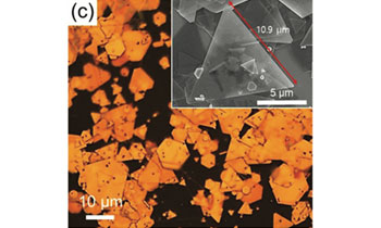
2D Single?Crystalline Copper Nanoplates as a Conductive Filler for Electronic Ink ApplicationsLee, J. W., Han, J., Lee, D. S., Bae, S., Lee, S. H., Lee, S. K., Moon, B. J., Choi, C. J., Wang, G., & Kim, T. W. (2018), Small, 14(8), 1703312.
Large-scale 2D single-crystalline copper nanoplates (Cu NPLs) are synthesized by a simple hydrothermal method. The combination of a mild reductant, stabilizer, and shape modifier allows the dimensional control of the Cu nanocrystals from 1D nanowires (NWs) to 2D nanoplates. High-resolution transmission electron microscopy (HR-TEM) reveals that the prepared Cu NPLs have a single-crystalline structure. From the X-ray photoelectron spectroscopy (XPS) analysis, it is found that iodine plays an important role in the modification of the copper nanocrystals through the formation of an adlayer on the basal plane of the nanoplates. Cu NPLs with an average edge length of 10 μm are successfully synthesized, and these Cu NPLs are the largest copper 2D crystals synthesized by a solution-based process so far. The application of the metallic 2D crystals as a semitransparent electrode proves their feasibility as a conductive filler, exhibiting very low sheet resistance compared to Cu NWs and a transmittance near 75%. The efficient charge transport is due to the increased contact area between each Cu NPL, i.e., so-called plane contact (2D electrical contact). In addition, this type of contact enhances the currentcarrying capability of the Cu NPL electrodes, implying that the large-size Cu NPLs are promising conductive fillers for printable electrode applications.
-
2020 ~ 2024
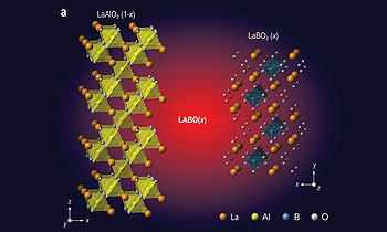
Electromagnetic Functionalization of Wide?Bandgap Dielectric Oxides by Boron Interstitial Doping.Park, D. S., Rees, G. J., Wang, H., Rata, D., Morris, A. J., Maznichenko, I. V., Ostanin, S., Bhatnagar, A., Choi, C. J., ... & McConville, C. F. (2018), Advanced Materials, 30(39), 1802025.
A surge in interest of oxide-based materials is testimony for their potential utility in a wide array of device applications and offers a fascinating landscape for tuning the functional properties through a variety of physical and chemical parameters. In particular, selective electronic/defect doping has been demonstrated to be vital in tailoring novel functionalities, not existing in the bulk host oxides. Here, an extraordinary interstitial doping effect is demonstrated centered around a light element, boron (B). The host matrix is a novel composite system, made from discrete bulk LaAlO3:LaBO3 compounds. The findings show a spontaneous ordering of the interstitial B cations within the host LaAlO3 lattices, and subsequent spin-polarized charge injection into the neighboring cations. This leads to a series of remarkable cation-dominated electrical switching and high-temperature ferromagnetism. Hence, the induced interstitial doping serves to transform a nonmagnetic insulating bulk oxide into a ferromagnetic ionic?electronic conductor. This unique interstitial B doping effect upon its control is proposed to be as a general route for extracting/modifying multifunctional properties in bulk oxides utilized in energy and spin-based applications.